Building the M17 Nokia 3310
Posted on 2025-06-29!!! WARNING - PLEASE READ !!!
- Before you order anything, please read the full article.
- Don’t be me. Just order the assembled board from PCBWay. It’s much easier and you support the M17 project.
- Many of the SMD parts are tiny. REALLY tiny. I’ve now learned what 0402 means in this context.
- If you decide to solder it by yourself, consider also ordering a stencil and reflow solder it. It’s a miracle that I got it working the way I did it.
- Only solder the SA868S module to the PCB after you are sure everything is fine. I was lucky - but if I had to build a second board, I would have had to either desolder or buy it again.
- You can’t send messages with the M17 3310 via an MMDVM hotspot. You need a packet mode compatible hotspot like the CC1200
After Wojciech SP5WWP posted on LinkedIn that you can now order pre-assembled PCBs for the M17-3310 project on PCBWay, I took a closer look at the project. This is a circuit board that can be installed in an old Nokia 3310 instead of the original mainboard. This board enables FM/FSK/M17 communication on the 70cm band and turns the good old 3310 into an interesting toy in conjunction with the M17 project. Currently there is a simple firmware that provides M17 messaging support with T9 text entry method. “The device can be powered with original Nokia lithium-ion batteries or their replacements and is able to charge them through the USB-C port. A UART USB interface is available, allowing the device to work as an RF modem.”
Sourcing
I have to admit that I didn’t understand PCBWay’s ordering process, so I decided to just order the bare PCB from JLCPCB, who I’ve had good experiences with so far. To do this, I downloaded the Gerber files here and used them to have 5 PCBs manufactured by JLCPCB.
I then downloaded the BOM from the same site and ordered almost all the necessary components from Mouser. The only component not available there is the G-NiceRF SA868S UHF RF module to which the OpenRTX firmware will be flashed later. I was able to order it from AliExpress.
Last thing missing is of course a Nokia 3310 or 3330. As I didn’t own either model, i bought both a 3310 and a 3330 second-hand. Of course, one phone is enough, but one of the two was so cheap that I had to go for it.
Here the full shopping list:
- A Nokia 3310 or 3330 with a functional display and keypad
- A G-NiceRF SA868S UHF RF module (AliExpress)
- All the components from the Bill of Materials (BOM)
- A PCB manufactured from the above mentioned Gerber files with a thickness of 1mm
I’ve mirrored the zip file from PCBWay here on my server. It includes the Gerber files, the BOM and more.
Nokia Disassembly
When I dismantled the Nokia, I realized how ingenious the basic idea of the project is and how great the phones of the 2000s were built.
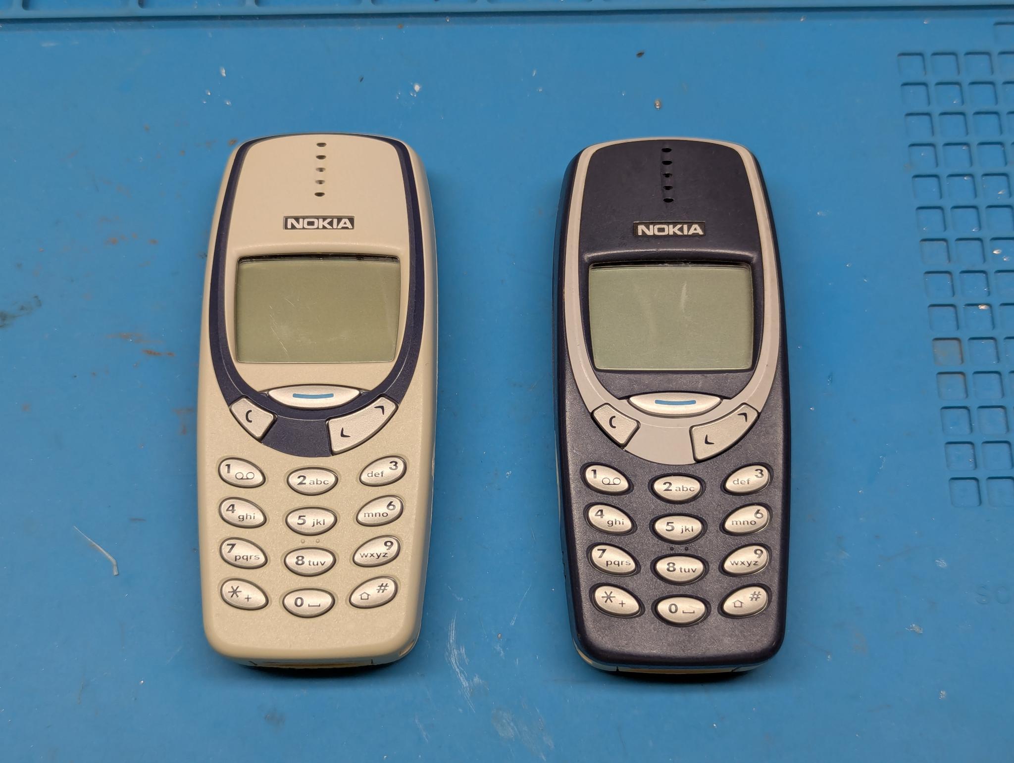
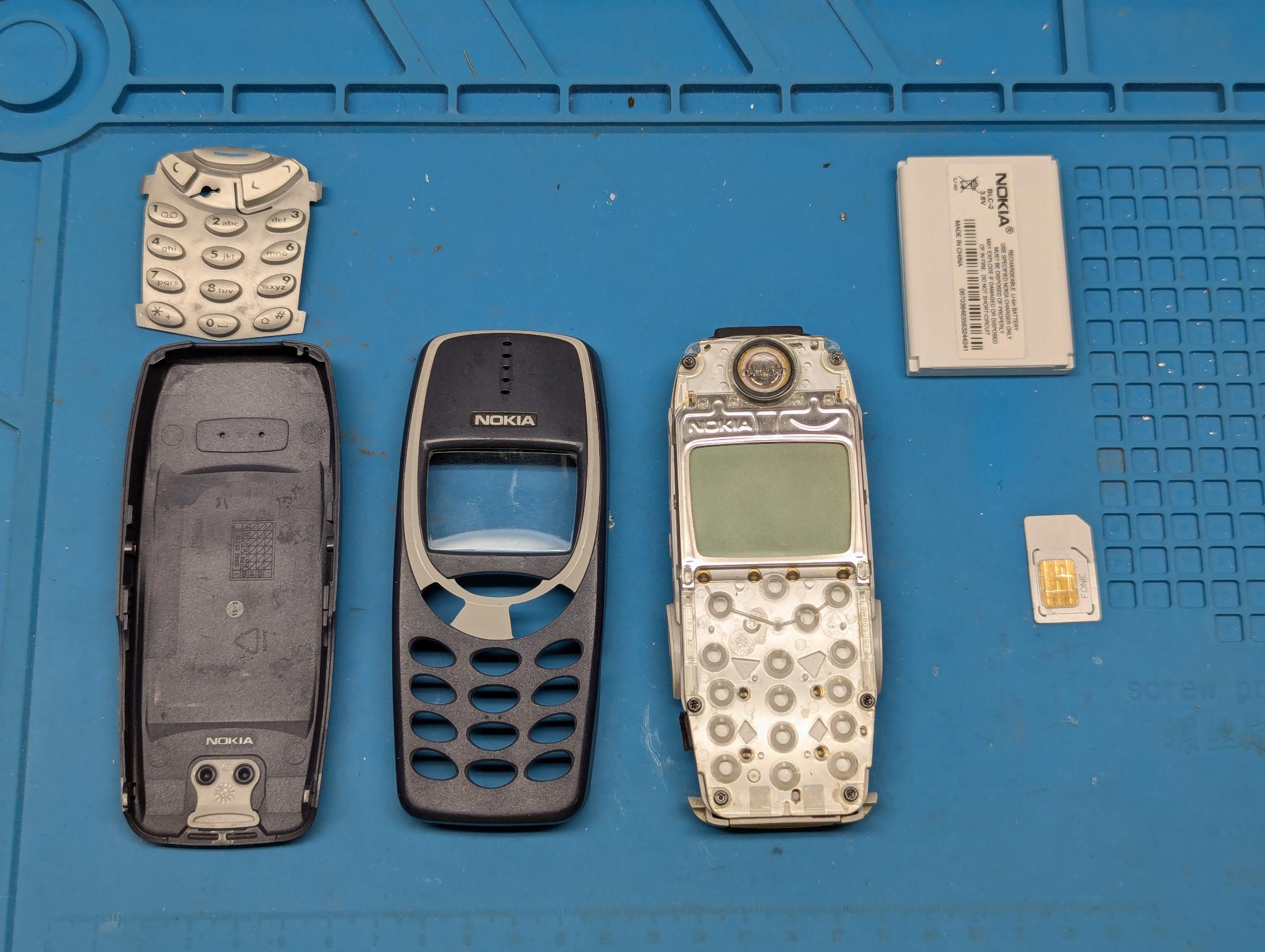
Here is a picture of both devices unopened:
First remove the rear cover by pressing the lower button on the back and pushing up the cover:
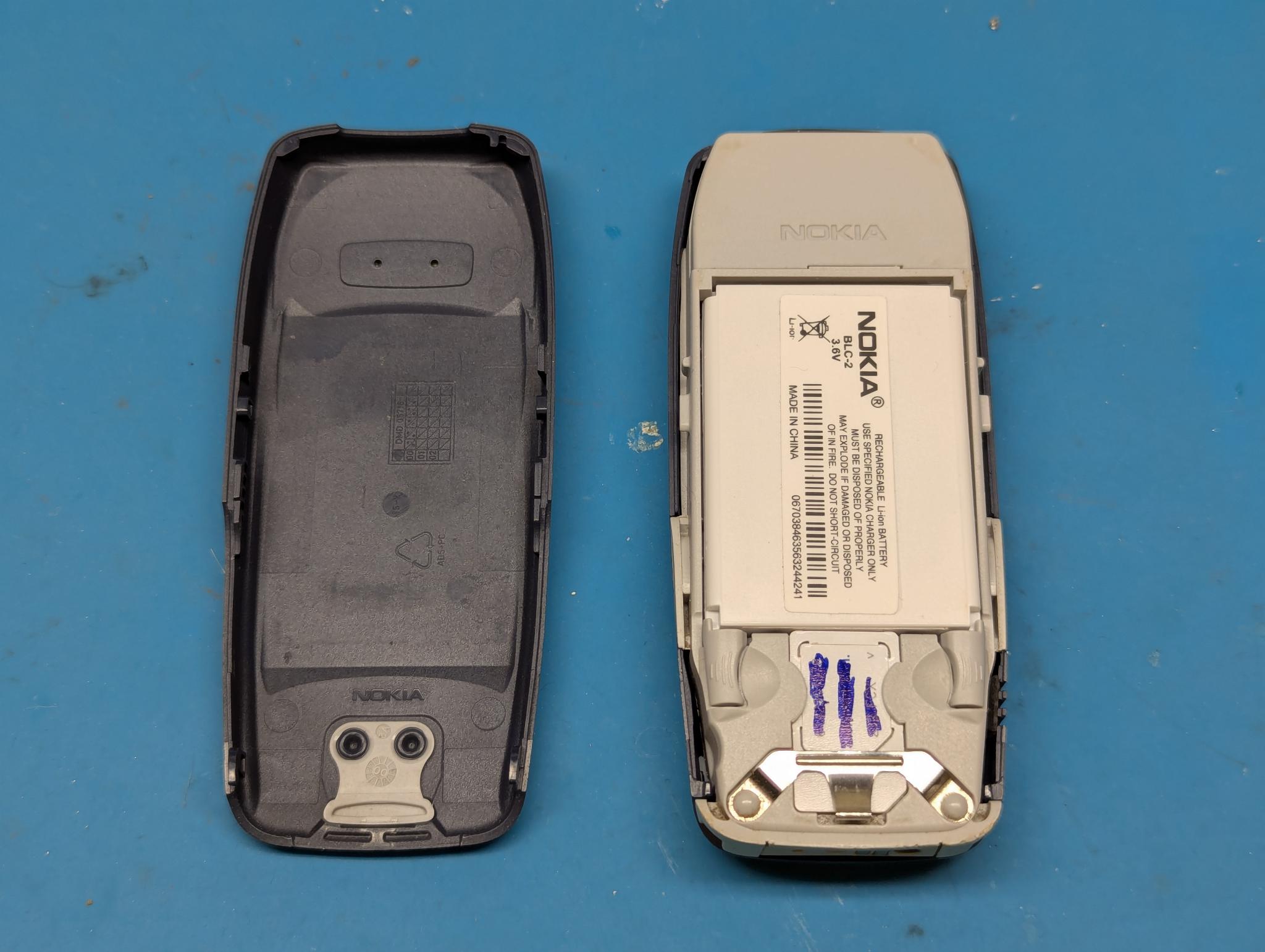
Then the battery and SIM card can be removed:
The front cover can then be removed by simply levering it off to the side. The keyboard foil will fall out:
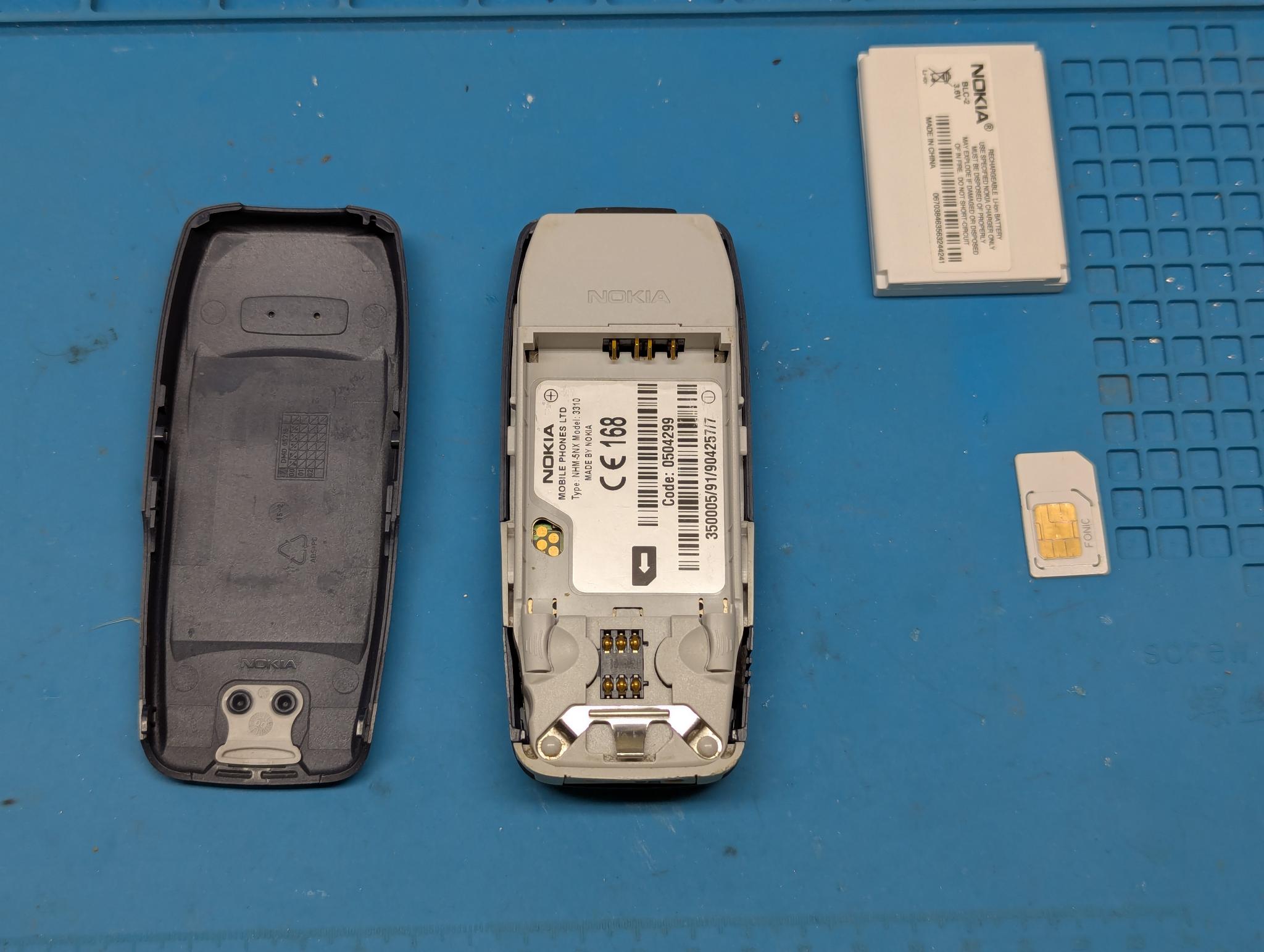
Now the PCB can be removed from the module above by loosening the 6 Torx T6 screws:
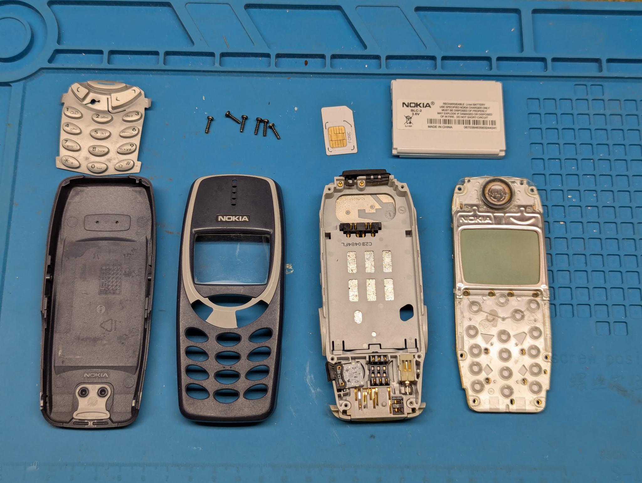
Here is a final picture of all the components in the order in which they are assembled:
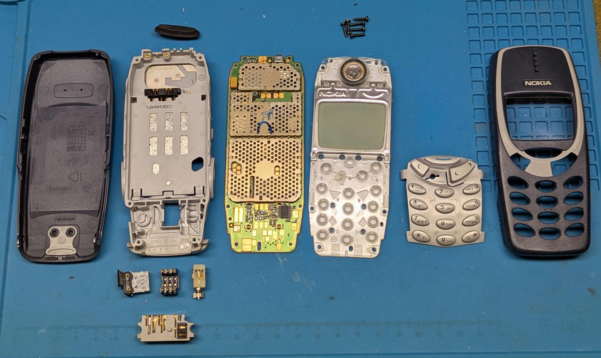
It is easy to see that apart from the 6 Torx screws, everything is not only modular but also connected to each other without screws and cables by spring contacts. In the past, if only the vibrator broke, for example, it was very easy to replace it. Unfortunately, those days are over.
Preparations
Before I would be able to solder, I first had to find out which components go where. First of all, I created a list of all the components based on the downloaded BOM:
| Designator | Value | Description |
|---|---|---|
| C1, C2 | 6p8 | Unpolarized capacitor |
| C10, C12, C13, C19, C5, C6, C7, C8, C9 | 100n | Unpolarized capacitor |
| C11, C17, C18 | 47uF/10V | Polarized capacitor |
| C14, C15, C16 | 10uF/10V | Polarized capacitor |
| C20 | 10n | Unpolarized capacitor |
| C21, C22 | 20p | Unpolarized capacitor |
| C3, C4 | 2u2 | Unpolarized capacitor |
| D1, D2, D3, D4, D8 | BAT60A | 10V 3A High Current Recitifier Schottky Diode, SOD-323 |
| D10, D11, D12, D13, D5, D6, D7, D9 | RED | Light emitting diode |
| FB1, FB2, FB3 | Bead | Ferrite bead |
| FL1 | LFCN-490+ | 490MHz 50 Ohm Passive Low Pass Filter, FV1206 |
| J8 | USB C | USB 2.0-only 16P Type-C Receptacle connector |
| L1 | 1u5 | Inductor |
| Q1, Q3, Q4, Q5, Q7 | BSS138 | 50V Vds, 0.22A Id, N-Channel MOSFET, SOT-23 |
| Q2, Q6 | IRLML6401 | -4.3A Id, -12V Vds, 50mOhm Rds, P-Channel HEXFET Power MOSFET, SOT-23 |
| R1, R6 | 22k | Resistor |
| R10, R13, R15, R17, R20, R7, R8 | 100k | Resistor |
| R11, R12, R18, R3, R31, R32, R33, R34, R35, R4, R9 | 47k | Resistor |
| R14, R28 | 1k | Resistor |
| R16, R19, R21, R22, R23, R24, R25, R26, R27 | 56R | Resistor |
| R2 | 2k2 | Resistor |
| R29, R30 | 5k1 | Resistor |
| R5 | 10k | Resistor |
| SW1 | POWER ON/OFF | |
| U1 | STM32F405RGTx | STMicroelectronics Arm Cortex-M4 MCU, 1024KB flash, 192KB RAM, 168 MHz, 1.8-3.6V, 51 GPIO, LQFP64 |
| U3 | MAX1555 | |
| U4 | MAX16054 | |
| U5 | TPS63031DSK | Buck-Boost Converter, 1.8-5.5V Input Voltage, 1A Switch Current, Adjustable Output Voltage, VSON-10 (DSK0010A) |
| U6 | USBLC6-2SC6 | Very low capacitance ESD protection diode, 2 data-line, SOT-23-6 |
| Y1 | 8MHz | Four pin crystal, GND on pins 2 and 4 |
The first hurdle I encountered was that I couldn’t find any documentation on where to place which components on the PCB. Wojciech then pointed out to me that this information can be found in the KiCad project files, which are part of the project on GitHub.
One big advantage of doing this project is that I learned some new things about KiCad. In this case I’ve learned that there is a plugin available, that creates an interactive HTML BOM viewer. The version I’ve created can be found here on my server. You might want to click on “F” on the top right as there will be no components placed on the back of the PCB.
Flashing the SA868S UHF module
The replacement board needs to be flashed twice: The first component that needs a firmware is the SA868S RF module, the second one the actual microcontroller. In this step, we will flash the RF module.
Download and install the rl78flash utility. How you install it, depends on your operating system. For me it was sufficient to download the latest release for macos and unpack the content.
Now download the latest OpenRTX firmware for the SA868S UHF module. Here is an example for version 1.4.1:
# cd ~/Downloads
# wget https://github.com/OpenRTX/sa8x8-fw/releases/download/v1.4.1/sa8x8-fw-sa868s-uhf.s37
We now have the software and firmware in place but we need to build a small programming adapter. I’ve done this with a UART to USB converter, two 1N5819 diodes, some wire and a small PCB. Here’s a diagram showing how it is connected:
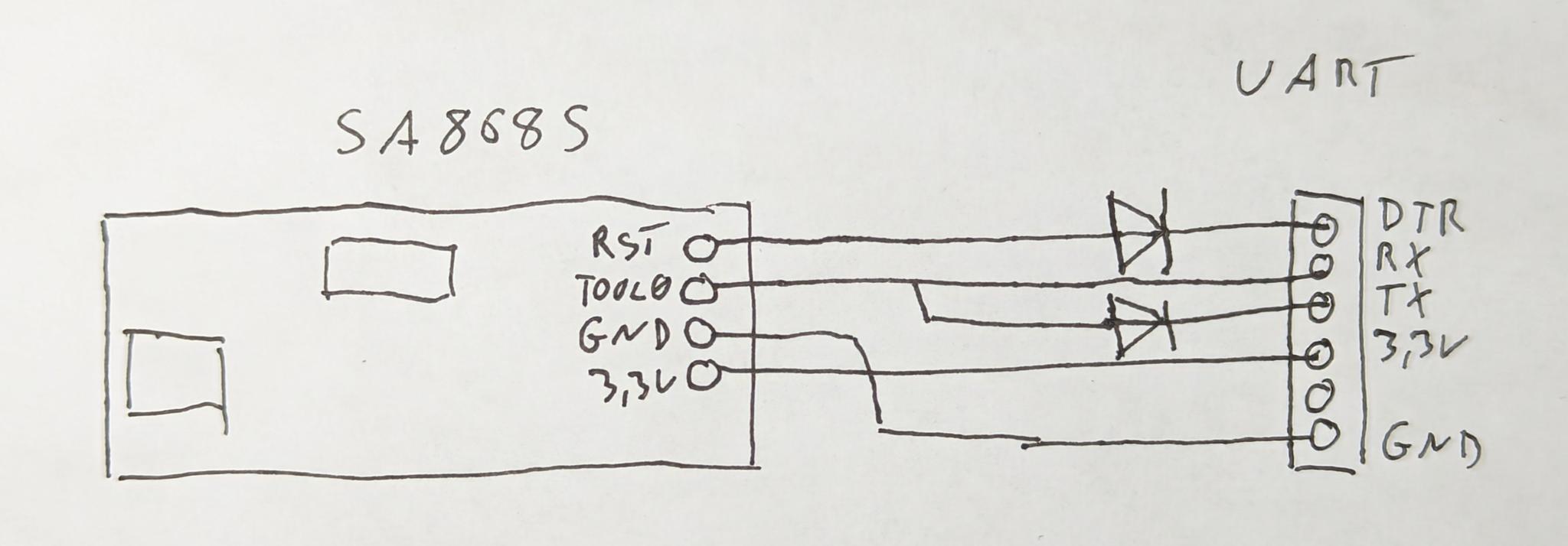
Here is how my version of this simple circuit looks like:
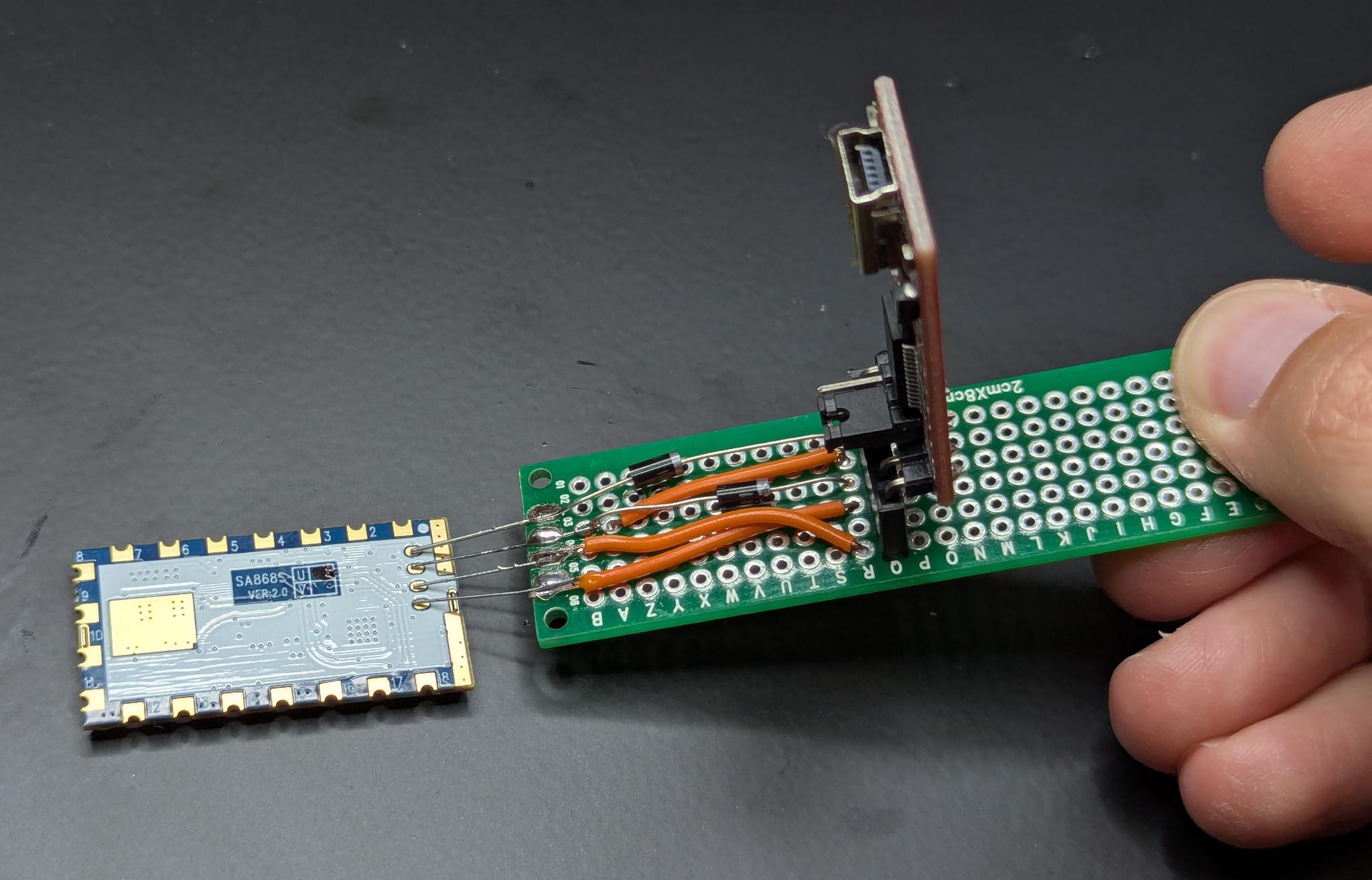
I’ve cut and soldered the legs of some resistors to the front of the PCB and bent them to the spacing of the four pins of the SA868S. The rest is quite self-explainatory.
To flash the firmware, plug in the UART to USB converter, hold the board with the four pins to the SA868S module and execute the following command.
Note: Make sure to jumper the converter to 3.3V!
# cd ~/Downloads/rl78flash/
# flash % ./rl78flash -m 1 -a -v /dev/tty.usbserial-A50285BI ~/Downloads/sa8x8-fw-sa868s-uhf.s37
rl78flash v0.7.0
Protocol configuration: protocol=0, code_block=1024, data_block=1024
Erase code flash
Erase data flash
Read file "/Users/rz01/Downloads/sa8x8-fw-sa868s-uhf.s37"
Write code flash
Write data flash
Verify Code flash
Verify Data flash
Reset MCU
I’ve chosen flash mode 1 (-m 1) as my UART to USB converter has a DTR pin. You might need to wire your adapter differently and then select another mode depending on your specific UART to USB board. Please consult this README and this diagram for more information on this.
The SA868S is now flashed. You can do this also after it has been soldered to the 3310-M17 board, I did it already before as I had to wait a while for the board to arrive.
Soldering the Board
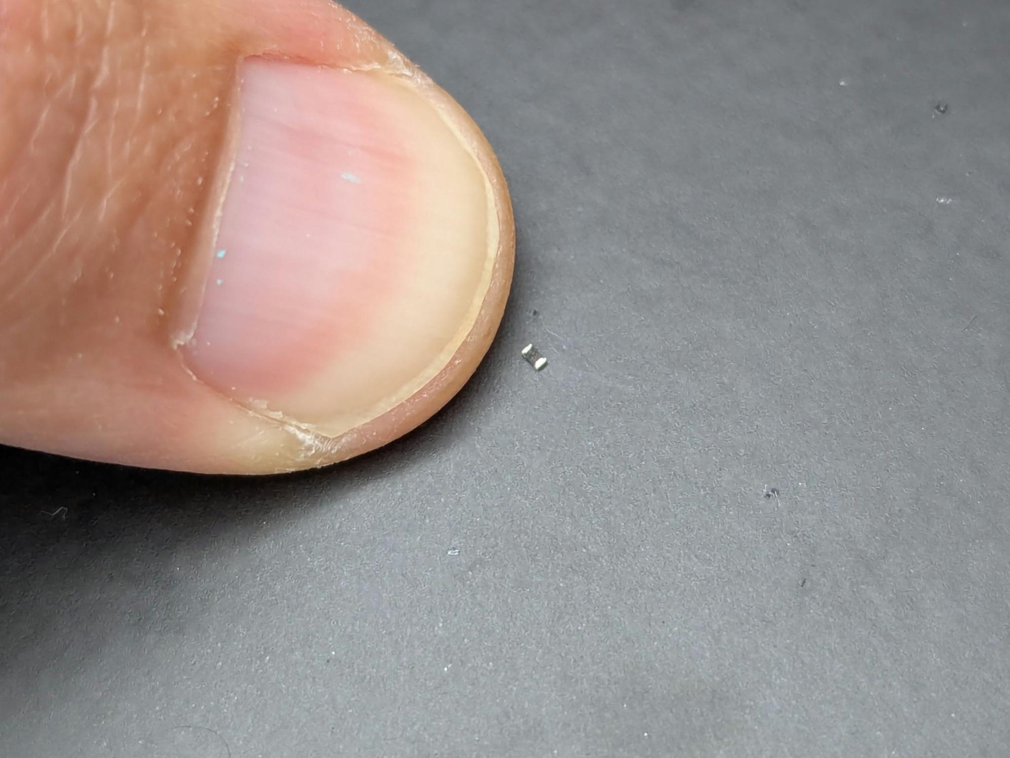
Soldering the SMD components by hand was a mistake. I should have done more research on the subject beforehand. The main problem is not even the tiny SMD components (0402):
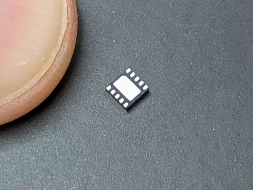
The real problem is the buck converter (U5) and the crystal (Y1). Both components do not have external legs but pads on the underside. Here is a close-up of U5:
I only realized this after I had soldered all resistors and small capacitors. After this work there was no way back for me. So I just put solder paste on the board without stencil, put the components on top and soldered with 190C hot air.
As expected, the board did not work. The day after this soldering drama I met SP5WWP in Friedrichshafen, who told me that some of my solder joints were rubbish. I had soldered them with 330C and a thin soldering tip. I already then noticed that I couldn’t get a good connection between the components and the GND pads.
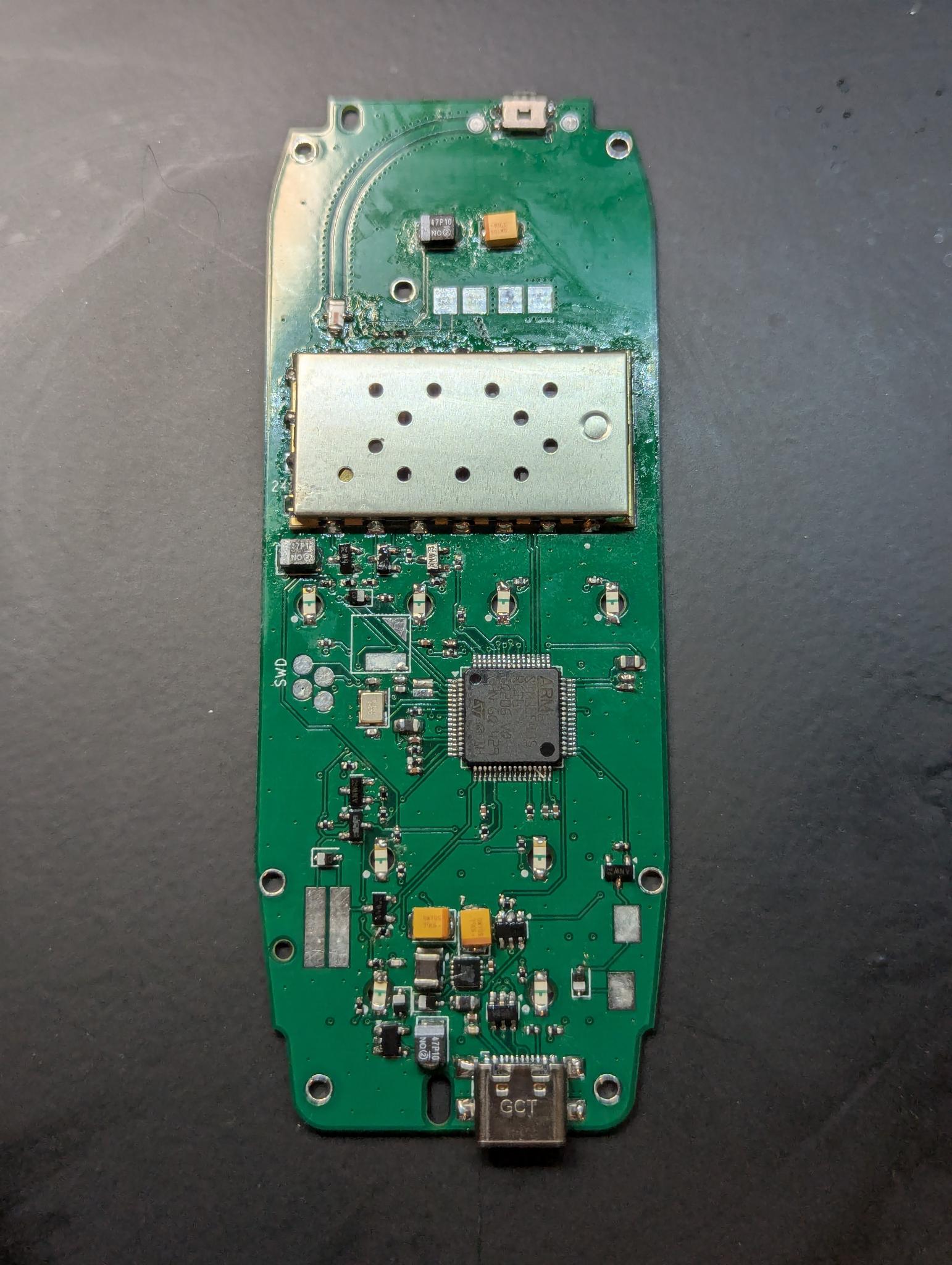
When I got back home, I re-soldered everything several times, but each time without success. The ST32 programmer did not recognize the board. Then I reached the point where I didn’t care anymore. So I practically drowned the board in flux and first soldered all the components with a soldering iron at 450C. Then I re-soldered U5 and Y1 with 450C hot air for quite a long time. This is what the board looked like after this torture (only half way cleaned):
Without any hope, I then connected the board to the computer and … WOW! It worked!
Now that the board is soldered including the already flashed RF module, one of the last tasks is to flash the microcontroller.
(Optional) Compiling the Firmware
You don’t need to compile the firmware by yourself as there are precompiled binaries available. But in case you want to adapt the software and compile it, this section explains the necessary steps.
Clone the firmware repository with all its submodules:
# git clone --recurse-submodules https://github.com/M17-Project/M17_3310-fw.git
To compile this firmware, you need to download and install the STM32CubeIDE first. You can find the installer package here.
Now start STM32CubeIDE, click on “File” > “Open Projects from File System…” and select the cloned directory.
Open the “Project Explorer” inside STM32CubeIDE
- right click on the topmost item (M17_3310-fw)
- select “Properties”
- under “C/C++ Build” select “Settings”
- click on “MCU/MPU GCC Compiler” > “Include Paths”
- make sure that the following paths are included:
../Core/Inc
../Core/libm17
../Drivers/STM32F4xx_HAL_Driver/Inc
../Drivers/STM32F4xx_HAL_Driver/Inc/Legacy
../Drivers/CMSIS/Device/ST/STM32F4xx/Include
../Drivers/CMSIS/Include
../USB_DEVICE/App
../USB_DEVICE/Target
../Middlewares/ST/STM32_USB_Device_Library/Core/Inc
../Middlewares/ST/STM32_USB_Device_Library/Class/CDC/Inc
Right click again the topmost item (M17_3310-fw), then select “Build Configurations” > “Set active” and decide between “Debug” and “Release”.
Now you can build everything with “Build Project”.
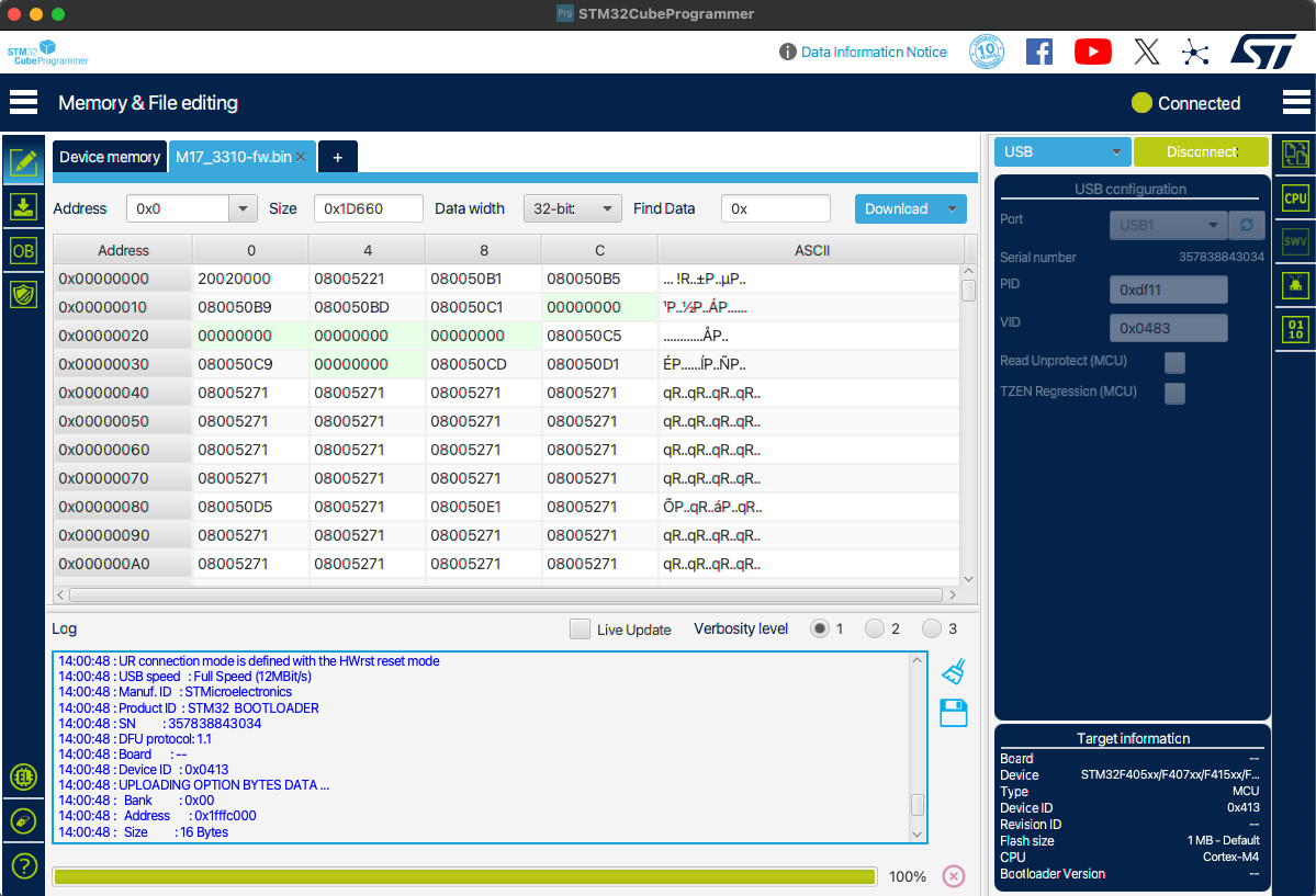
Flashing the Microcontroller
To flash the microcontroller with the firmware, download and install STM32CubeProgrammer. It is available here for Mac/Lin/Win.
First of all, set the M17-3310 board to USB DFU mode:
- Open the application STM32CubeProgrammer
- Switch from “ST-LINK” to “USB” inside the dropdown box left to “Connect”
- Plug in the USB cable and connect your M17-3310 board with your computer
- Press and hold the OK button (large horizontal one with a blue bar, just below the display)
- Press the power button at the top of the device
- Release the OK button
The device should now enter USB DFU mode and ready to be connected.
To flash the firmware, do the following:
- Select the firmware file (M17_3310-fw.bin)
- Click on “Refresh”. Something like “USB1” should appear in the “Port” combobox
- Click on “Connect”
- Click on the blue “Download” button
The STM32 now gets flashed.
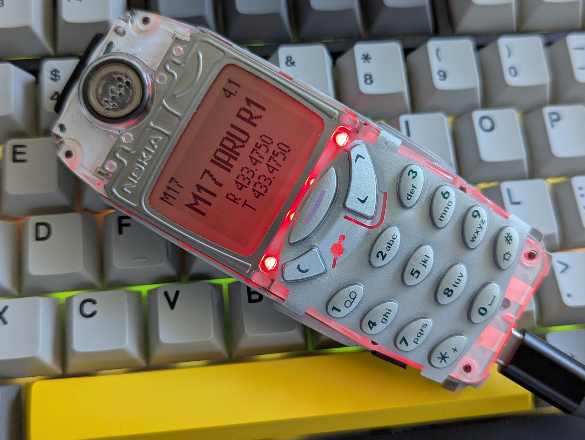
Afterwards, click “Disconnect”, remove the USB cable and power on your Nokia:
Reassembly
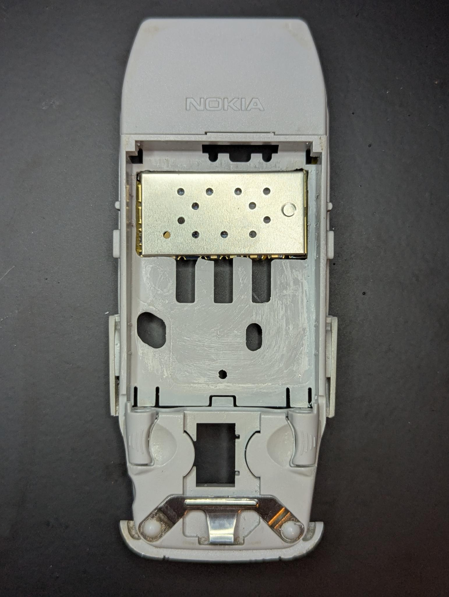
Before the Nokia can be reassembled, you need to cut out a SA868S sized rectangular hole into the middle plastic part that holds the battery. The reason for this is that the RF module is a bit too thick to fit between the PCB and the inner plastic shell. Cutting the plastic is easy at it is a very soft material:
After this small modification, the Nokia can the reassembled. Make sure to not install the old power socket module at the bottom of the phone as we now have a USB-C port directly on the PCB.
Conclusion
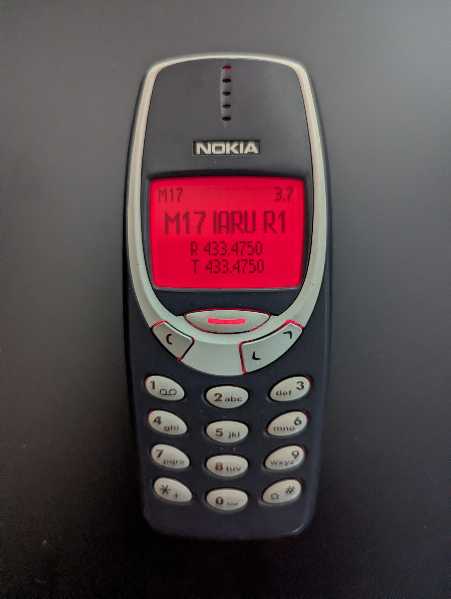
This is what the modified and reassembled Nokia looks like:
Would I do it again the exact same way? Absolutely not! Was it exciting, rewarding and educational? Oh yes!
I am looking forward to further expirements with the M17 Nokia but for now the result is very satisfying. This is the first self-build project with an outstanding build quality - which is of course Nokia’s merit. The 3310 has always been great and this version is great in a different way.
Now I just have to build a CC1200 hotspot - but with stencil, solder paste and a hot plate.
Big thanks to Wojciech for this project and all the help with finishing my build!